Van der Waals heterostructure fabrication
The van der Waals heterostructures (VdWh) are vertical stacks of thin crystal layers (typically mono – layers) [1], as illustrated in Figure 1.
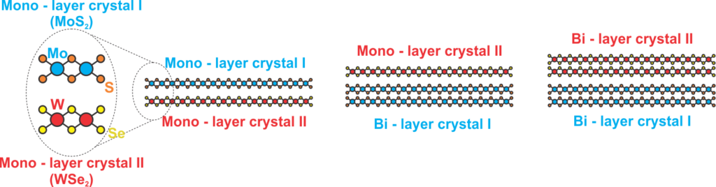
Figure 1. An illustration of VdWhs built from thin TMD crystal layers of various thickness.
In PV-Waals, VdWhs are built from thin layers of semiconducting transition metal dichalcogenides (TMD), such as MoS2, WS2, MoSe2 and WSe2 (see Figure 1). As an example, Figure 2 shows an optical microscopy image of a VdWh formed by stacking small MoS2 monolayers on top of large WS2 monolayers. The MoS2, and WS2 monolayers were grown on SiO2/Si substrates using chemical vapor deposition, and provided by our collaborators from the Center of Excellence for Advanced Materials and Sensing Devices, Institute of Physics, Zagreb, Croatia.
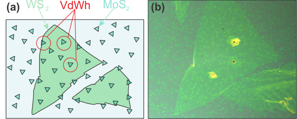
Figure 2. (a) A sketch illustrating the VdWh formed from small MoS2 monolayer triangles and large WS2 monolayers. (b) Corresponding optical microscopy image.
The fabrication of VdWhs, such as those from Figure 1, is based on transferring layers of already prepared thin TMDs one on top of the other thin TMDs [2]. Two complementary transfer variants, namely the wet transfer method (WTM) and the dry transfer method (DTM), will be used for VdWh fabrication in PV-Waals.
- The wet transfer method is typically used for creating large-area VdWh, which are based on CVD grown 2D materials. The wet transfer procedure consists of lifting a CVD grown TMD and transferring it on top of another CVD grown TMD. The lifting and the transfer are done using a substrate etchant / intercalant solution and a supporting Polydimethylsiloxane (PDMS) film [3]. The key steps of the wet transfer method are illustrated in Figure 3(a).
- The dry transfer method is used for fabricating high quality, microscopic VdWh, whose constituent layers are obtained by micromechanical exfoliation. In this method, the TMD flakes are directly exfoliated on the PDMS films and then transferred on top of other, previously prepared TMD flakes which lie on a carrier substrate. The key steps of the dry transfer method are illustrated in Figure 3(b). Unlike the wet transfer method, the dry transfer does not involve usage of any kind of substrate etchants yielding heterostructures of better quality with less contaminants.
For precise alignment of microscopically small, exfoliated TMD flakes a specialized transfer equipment is necessary [2]. Figure 4 shows the dry transfer setup, which consists of a microscope and two positioning stages. The microscope is used for identification of the TMD flakes resting on both PDMS and the carrier substrate, while the two stages are used for achieving precise alignment of the flakes. In fact, steps 3 and 4 from Figure 3(b), are done using the dry transfer setup.

Figure 3. Illustration of (a) wet transfer method and (b) dry transfer method.
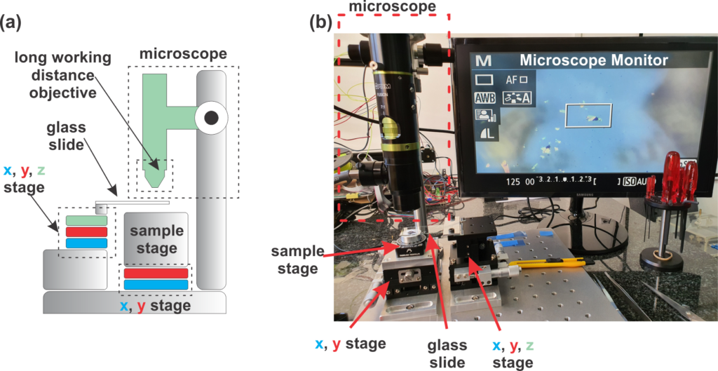
Figure 4. The dry transfer setup: (a) sketch and (b) the actual setup.
[1] K.S. Novoselov, A. Mishchenko, A. Carvalho, A. H. Castro Neto, “2D materials and van der Waals heterostructures”, Sicence 353, aac9439-1 (2016)
[2] R. Frisenda, E. Navarro-Moratalla, P. Gant, D. Perez De Lara, P. Jarillo-Herrero, R. V. Gorbachev, “Recent progress in the assembly of nanodevices and van der Waals heterostructures by deterministic placement of 2D materials”, A. Castellanos-Gomez, Chem. Soc. Rev., 47 , 53 (2018)
[3] I. Niehues, A. Blob, T. Stiehm, R. Schmidt, V. Jadriško, B. Radatović, D. Čapeta, M. Kralj, S. M. de Vasconcellos, R. Bratschitsch, “Strain transfer across grain boundaries in MoS2 monolayers grown by chemical vapour deposition”, 2D Mater. 5, 031003 (2018)