Overview
PV-Waals addresses solid-state physics, nanoelectronics, plasmonics, nanotechnology and related fields. The project activities can be classified into three categories, as depicted in Figure 1. A smaller part of the effort is devoted to Theory. It involves the use of theoretical and numerical methods for the purpose of designing and analyzing the plasmonic nanoparticle arrangement which will enhance the light absorption in the nanometer thin vdWh photovoltaics. Fabrication involves activities such as substrate and thin film preparation, van der Waals heterostructure fabrication and transfer, deposition of electrical contacts and plasmonic nanoparticles. Its ultimate aim is to produce the nanometer thin plasmonically enhanced vdWh photovoltaic device which is also the ultimate scientific objective of PV-Waals. Characterization includes a number of experimental techniques used for the purpose of probing the characteristics of produced samples.
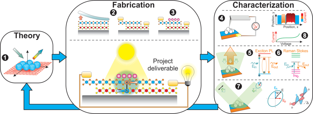
Figure 1. Project overview.
Theory
This category of project activities consists of the task called Theoretical design and numerical modeling (Task 1) and is indicated by “1” in the Theory bubble in Figure 1. Its aim is to understand and efficiently model how film-coupled plasmonic nanoparticles modify the absorption of light in the vdWh layer by rigorously solving macroscopic Maxwell equations in which light interaction with two- and three-dimensional media is described by dielectric susceptibilities. In doing so, we assume that the optical properties of individual 2D crystals [1] remain invariant when combined into vdWhs. While this assumption does not account for the change in vdWh absorption due to the charge-transfer exciton formation, recent experiments [2] have demonstrated a fairly good agreement with absorption calculated under these assumptions.
Fabrication
The Fabrication activities involve two tasks, associated with vdWh preparation by 2D crystal transfer techniques with subsequent contact fabrication (Task 2) and the fabrication of light trapping structures (Task 3).
VdWh device fabrication (Task 2)
The target vdWh photovoltaic device depicted in Figure 2(a) involves a vertical vdWh formed between two different 2D semiconductors on top of several substrate types. The project focuses primarily on transition metal dichalcogenides (TMDCs) such as MoS2, WS2, MoSe2 or WSe2, as they have so far been proven [3] most promising for photovoltaics because of type II band alignment. The first step of vdWh fabrication is the preparation of 2D crystals. In this project, two complementary methods are used: in-house mechanical exfoliation (ME) and chemical vapor deposition (CVD). ME is a process involving the use of an appropriate scotch tape for peeling 2D crystal sheets from large (millimeter size) single crystals [4], yielding the highest quality single crystal flakes, typically few tens of micrometer in size. CVD grown 2D crystals are provided by our collaborators. VdWhs are formed by lifting TMDC 2D crystals from initial supporting substrates and stacking them onto a convenient substrate or on top of another 2D crystal, Figure 2(b). Two complementary transfer methods are used: the wet transfer method for large-area CVD grown TMDCs [5] and the dry transfer method for small-area mechanically exfoliated TMDCs [6]. In order to achieve a microscopic precision in stacking 2D crystals prepared by ME, the project also involves building of a specialized dry transfer setup, depicted schematically in Figure 2(c). This setup involves a microscope with a long working distance objective, a glass slide and several micropositioning stages for precise alignment [7]. The final step of vdWh device fabrication is the creation of electrical contacts, as shown in Figure 2(b). For the purpose of obtaining ohmic contacts with minimal resistance, various metals and their combinations, including Au, Ti and Cr, will be considered [8].
Fabrication of film-coupled plasmonic nanoparticles (Task 3)
Nanometer thin dielectric films for fine-tuning the film-coupled plasmonic nanoparticle properties are prepared on top of various substrates (SiO2, Au, Al, Ag) by using layer-by-layer polyelectrolyte deposition [9] which is well-known for allowing the very precise distance control between underlying metal films and plasmonic nanoparticles [10]. Optical quality metal films (Au, Al, Ag), acting as substrates for polyelectrolyte films are prepared by our collaborators. Two types of plasmonic nanostructures are considered: colloidal nanoparticles of various shape and size distribution and metal island films prepared by electron beam evaporation. In case of colloidal nanoparticles, the plasmonic properties are controlled by choosing appropriate colloids (monodisperse, polydisperse, combining various shapes) whose deposition onto the surface of thin films (including vdWhs) is controlled by surface activation (sulfurization or use of appropriate surfactants, e.g. polyvinylpyridine). In case of metal island films, the sample temperature, deposition speed and total mass determine the characteristics of the ensemble [11].
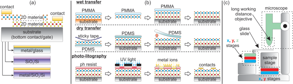
Figure 2. Overview of Fabrication activities.
Characterization
The characterization activities involve five tasks each focused on a specific aspect of the vdWh photovoltaics physics. Together, these tasks will provide a complete picture of the vdWh device characteristics and the mechanism of plasmonic enhancement.
Local electrical and photovoltaic properties (Task 4)
AFM based electrical methods are employed to characterize the spatial distribution of electrical surface potential and currents in dark and under illumination with nano-scale resolution. For that purpose, Kelvin probe force microscopy (KPFM), electric force microscopy (EFM), and conductive AFM (C-AFM) is used. As our instrument (NTMDT NTEGRA Prima with confocal Raman spectrometer) currently does not provide the option of a controlled external sample illumination, a setup for light-assisted AFM measurements (to be attached to our ambiental system) will be build within PV-Waals. This will allow us to assess the characteristics of fabricated nanometer thin solar cells by measuring surface photovoltage, short-circuit current and open-circuit voltage.
Photoluminescence quantum yield assessment (Task 5)
The fabrication of high quality heterojunctions is absolutely necessary for attaining high quality vdWh based photovoltaic devices. The quality of fabricated heterojunctions will be inspected by monitoring the heterojunction photoluminescence (PL) and assessing the corresponding PL quantum yield (PLQY). The selected heterojunctions with the highest PLQY values will be subsequently subjected to the external voltage, applied between the fabricated contacts, in order investigate its influence on both the excitonic transitions, which dominate the PL, and PLQY.
Raman and low-temperature PL spectroscopy (Task 6)
Raman spectroscopy can provide information on number of layers, defects, strain and doping of 2D TMD materials through subtle changes in the positions, linewidths and relative intensities of the peaks present in Raman spectra. This method will be employed for characterization of the fabricated structures in PV-Waals, but also for the study of the interaction of phonons with charge carriers. Low temperature PL spectroscopy is utilized for the study of diverse types of excitons present in vdWhs, since the reduction in temperature leads to the PL linewidth decrease and allows for observation of closely positioned exciton peaks. Low temperatures also allow for radiative recombination of excitons otherwise prevented by non-radiative decay through thermal processes.
Ellipsometric measurements (Task 7)
Due to its extreme surface sensitivity, spectroscopic ellipsometry (SE) is becoming a method of choice for verifying optical and structural properties of thin films in photovoltaics [12]. SE is routinely used for well defined thin films and surfaces. Here it is used for monitoring the layer-by-layer polyelectrolyte deposition. However, its use for studying inhomogeneous films made of plasmonic nanoparticles is more challenging. During the nanoparticle deposition phase, the focus of SE analysis will be on developing appropriate numerical models (together with Task 1) that allow for establishing an accurate connection between the collective behavior of randomly distributed nanoparticles (whose distribution will be determined by scanning electron microscopy) and measured ellipsometric response.
Plasmonically enhanced photovoltaic properties (Task 8)
I/V characteristics will be measured on bare 2D hetero-structures and ones with deposited metallic nanoparticles. In both cases, the samples will be illuminated by an external light. Due to localized surface plasmon resonances excited by the light, the nano-particles behave as nano-optical antennas with enhanced electric field in their vicinity. The electric field supports the generation of additional electron-hole pairs thus increasing overall absorption and electrical current in 2D hetero-structures [13]. Investigation of this electrical current enhancement provided by plasmonic nanoparticles will be the focus of this task.
References
- Y. Li et al., Phys. Rev. B 90, 205422 (2014)
- D. Jariwala et al., Nano Lett. 16, 5482 (2016)
- W. Liao et al., Appl. Mater. Today 16, 435 (2019)
- K.S. Novoselov et al., PNAS 102, 10451 (2005)
- J. Mlack et al., Sci. Rep. 7, 43037 (2017)
- R. Frisenda et al., Chem. Soc. Rev. 47, 53 (2018)
- A. Castellanos-Gomez et al., 2D Mater. 1, 011002 (2014)
- D. S. Schulman et al., Chem. Soc. Rev. 47, 3037 (2018)
- G. Decher, Science 277, 1232 (1997)
- J.J. Mock et al., Nano Lett. 8, 2245 (2008)
- M. Loncaric, J. Sancho-Parramon, H. Zorc, Thin Solid Films 519, 2946 (2011)
- H. Fujiwara, R. W. Collins, “Spectroscopic Ellipsometry for Photovoltaics, Volume 1”, Springer (2018)
- T. J. Echtermeyer et al., Nat. Comm. 2, 458 (2011)