Raman spectroscopy of van der Waals heterostructures
Raman spectroscopy is a versatile tool for study of microstructural properties of 2D semiconducting transition metal dichalcogenides (TMDs), such as number of layers, defects, doping, strain, electron-phonon interaction and many more [1, 2]. Changes in position, linewidth and relative intensities of vibrational peaks in the Raman spectra of TMDs give valuable insight into these properties. Raman characterization of 2D TMDs and van der Waals (vdW) heterostructures built from them can be used for the assessment of potential changes in crystalline structure, phase, layer orientation, defects, surface states and electron-phonon interaction induced by TMD layer stacking.
MoS2, both for 2H- and 3R-polytypes, has two Raman active vibrations, E’/E2g1 (in-plane), positioned at ~386 cm-1, and A1’/A1g (out-of-plane), positioned at ~405 cm-1, as shown in Figs 1(a) and 1(b). When the number of layers increases, interlayer van der Waals (vdW) forces suppress atomic vibrations and the out-of-plane A1’/A1g mode experiences a blue-shift [3]. The in-plane E’/E2g1 mode experiences a red shift as the number of layers increases. Thus, difference of these two phonon mode positions in MoS2 increases with the increase of the number of layers, having the largest value for bulk MoS2. This enables identification of the number of layers from the difference of two phonon mode wavenumbers.
WS2 has two first order Raman active modes, also E2g1 (in-plane) and A1g (out-of-plane), but when a resonant excitation of 514.5 nm or 532 nm is used, second order peaks, mainly acoustic phonons such as 2LA(M), become prominent due to phonon-exciton coupling [3], as shown in Fig. 1(a). When a non-resonant excitation line such as 488 nm is used, only first-order Raman modes appear in spectra of WS2, positioned at ~357 cm-1 and ~417 cm-1, Fig. 1 (b). Difference of E2g1 and A1g mode positions in WS2 is also correlated with the number of layers, but the mode positions can be unambiguously determined only when the second order peaks are absent from the spectra, i.e. when a non-resonant excitation line is used.
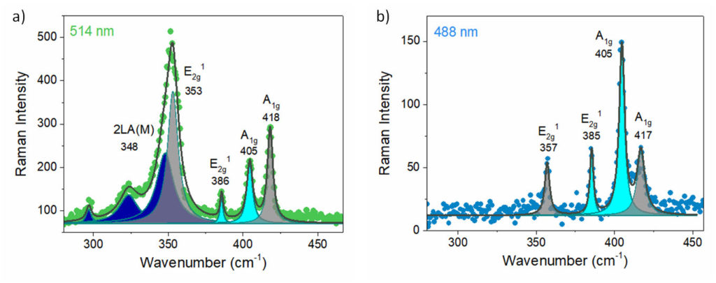
Figure 1. Raman spectrum of a MoS2/WS2 heterostructure obtained with 514.5 nm (a) and 488 nm (b) excitations. Experimental data is represented by green and blue circles and multi-peak Lorentzian fts to the data are represented by solid lines. Cyan shaded peaks represent MoS2 first-order Raman modes, grey shaded peaks are WS2 first-order Raman modes and blue shaded peaks represent second-order Raman modes of WS2.
When a vdW heterostructure MoS2/WS2 is formed, its Raman spectra should contain both MoS2 and WS2 Raman modes and changes that can happen as a result of stacking can be assessed through these vibrational features. Transfer of as-grown TMDs can induce shifts and broadening of their Raman peaks due to formation of inter-layer bonds or due to the occurrence of the impurities as a consequence of transfer method. Furthermore, in the spectra of van-der-Waals heterostructures new inter-layer modes can appear at very low wavenumbers representing the vibrations of entire layers1.
Continuity of the layers within vdW heterostructures, their homogeneity, presence of defects etc. can be assessed by mapping the Raman modes intensities of MoS2 and WS2 across the heterostructures, as shown in Figs 2(a,c), 3(a,c), 4(c). Number of layers within a MoS2 flake can be tracked by mapping of the difference of phonon mode positions of MoS2, Fig. 2 (d). In the case of MoS2 monolayer the difference between A1g and E2g1 mode wavenumbers varies between 17 cm-1 and 20 cm-1 depending on the synthesis method and increases for ~4 cm-1 approximately when going from monolayer to bilayer3. The following images present Raman maps of vertical heteostructures obtained from originally CVD-grown MoS2 and WS2 flakes on SiO2/Si substrates. MoS2 flakes were transfered onto substantially larger WS2 flakes using wet transfer technique.
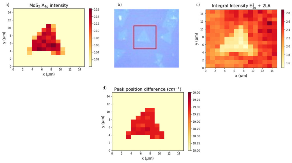
Figure 2. MoS2 triangular flake positioned over WS2 with its entire surface: Raman map of MoS2 A1g peak intensity (a), optical image (b) and Raman maps of integral intensity of E2g1 and 2LA modes of WS2 (c) and the difference of positions of E2g1 and A1g modes in MoS2 (d). Raman maps were obtained from 15 x 15 μm2 area.
Occasionally, edge effects can be observed, such as the increase of the intensity of Raman modes both in MoS2 and WS2 at some intersections of MoS2 flakes and WS2 edges, as shown in Figs 3 (a) and 3(c).
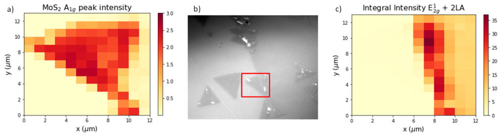
Figure 3. MoS2 flake positioned partly over WS2 flake and partly over SiO2/Si substrate: Raman map of MoS2 A1g peak intensity (a), optical image (b) and Raman map of Integral intensity of E2g and 2LA modes of WS2 (c). Raman maps were obtained from 12 x 13 μm2 area.
As mentioned above, A1g mode in MoS2 experiences blue shift with the increase of the number of layers, so the nucleation centers of flake growth which are thicker than the rest of the flake can be observed in a map of this peak’s position, Fig. 4 (a).
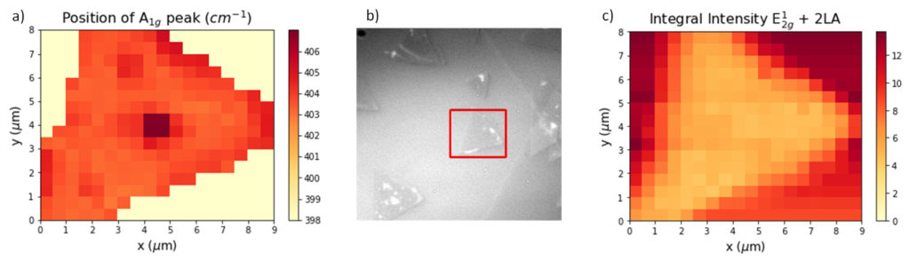
Figure 4. MoS2 layer positioned over WS2 with its entire surface: Raman map of MoS2 A1g peak position (a), optical image (b) and Raman map of integral intensity of E2g and 2LA modes belonging to WS2 (c). Raman maps were obtained from 9 x 8 μm2 area.
[1] X. Cong, X.-L. Liu, M.-L. Lin, and P.-H. Tan, “Application of Raman spectroscopy to probe fundamental properties of two-dimensional materials”, npj 2D Materials and Applications 4, 13 (2020).
[2] S. Zhang, N. Zhang, Y. Zhao, T. Cheng, X. Li, R. Feng, H. Xu, Z. Liu, J. Zhang, and L. Tong, “Spotting the differences in two-dimensional materials – the Raman scattering perspective”, Chem. Soc. Rev. 47, 3217 (2018).
[3] M. O’Brien, N. McEvoy, D. Hanlon, T. Hallam, J. N. Coleman, and G. S. Duesberg, “Mapping of Low-Frequency Raman Modes in CVD-Grown Transition Metal Dichalcogenides: Layer Number, Stacking Orientation and Resonant Effects”, Scientific Reports 6, 19476 (2016).