Photolithography and metal contact evaporation
Generally speaking, photolithography is utilized to define features at the micro/nano scale. Here, we demonstrate the fabrication of field effect transistors based on 5-10 µm channel length features with gold metallic contacts evaporated on top of two-dimensional (2D) materials.
The schematic overview of the photolithography and metal contact evaporation process is depicted in Figure 1. Initially, photoresist (e.g. AZ1505) is spin-coated on a substrate with 2D materials. The photoresist soft baking step follows prior to mask alignment and UV light exposure. Development of the exposed photoresist produces the desired features. Subsequently, metal contacts are evaporated and lift-off is performed in order to remove the photoresist and finalize the devices.
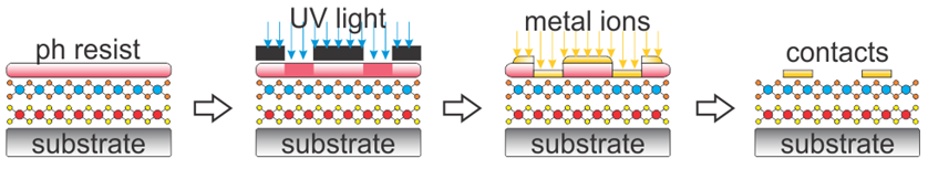
Figure 1. The schematic overview of the photolithography and metal contact evaporation process.
Two-dimensional materials considered in this work were produced by mechanical exfoliation of bulk crystals or via chemical vapor deposition (CVD). In particular, a few-layer graphene flake depicted in Figure 2(a) is the result of mechanical exfoliation, whereas the monolayer WS2 flake shown in Figure 2(c) was grown by chemical vapor deposition [1].
Recent work in this field attempted to elucidate the effects of metal contacts on monolayer transition metal dichalcogenides (such as MoS2/WS2) [2]. Metal contacts are considered to be a key limiting factor for the electronic performance of 2D semiconductor devices. Interestingly, 7 different metals with work functions between 3.1 eV and 5.2 eV were evaluated as contacts on monolayer MoS2 grown by CVD – nonetheless, optimal Ohmic contact performance is difficult to obtain and the findings demonstrate that titanium (Ti) reacts with MoS2, whereas gold (Au) generates a certain degree of damage to MoS2 [2]. A previous computational study had also shown that the most commonly used metal contact (Au) is rather inefficient for electron injection into single-layer MoS2. Further experimental and computational work is still required in order to understand the mechanisms that determine the electronic performance of 2D semiconductor devices with different metal contacts.

Figure 2. (a) A mechanically exfoliated few-layer graphene flake, (b) the identical flake with 25 nm thick Au contacts, (c) a CVD grown monolayer WS2 flake, and (d) a different monolayer WS2 flake with 15 nm thick Au contacts.
In this work, Au contacts were evaporated on top of a few-layer graphene flake and a monolayer WS2 flake after photolithography processing. Lift-off in acetone followed, resulting in back-gate field effect transistor structures shown in Figures 2(b) and 2(d). Hereby, the heavily doped silicon wafer acts as the back gate, while the photolithography-defined metal contacts act as the source/drain terminals. It should be noted that the WS2 flake depicted in Figure 2(c) is not identical to the flake in Figure 2(d). Furthermore, the channel length feature sizes in Figures 2(b) and 2(d) are approximately 10 µm and 5 µm, respectively.
[1] Samples with CVD grown WS2 flakes were provided by Davor Čapeta and Marko Kralj from the Institute of Physics in Zagreb, Croatia.
[2] K. Schauble et al. “Uncovering the Effects of Metal Contacts on Monolayer MoS2”, ACS Nano 14, 14798-14808 (2020).
[3] I. Popov et al. “Designing Electrical Contacts to MoS2: A Computational Study”, Phys. Rev. Lett. 108, 156802 (2012).