Modeling light scattering on plasmonic nanoparticle clusters
In order to increase the light absorption efficiency in nanometer thin van der Waals photovoltaics, we consider various plasmonic nanoparticles randomly distributed in the vicinity of the active layer. For purposes of modeling light scattering on nanoparticle ensembles deposited on layered substrates, we use two numerical approaches. The first is based on a commercial finite element method solver (COMSOL Multiphysics) suitable for modeling a smaller number of nanoparticles of completely arbitrary shape. The second is Smuthi (‘scattering by multiple particles in thin-film systems’), a freely available Python software for solving light scattering problems involving particles of various shapes near or within layered media, which is suitable for simulating large nanoparticle clusters.
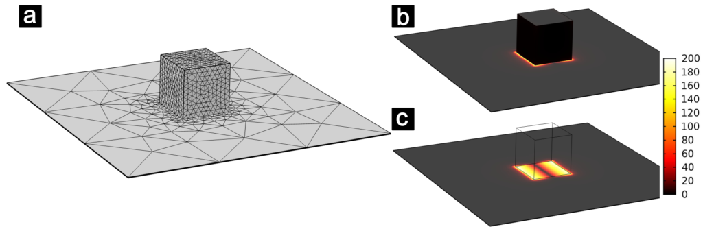
Figure 1. COMSOL Multiphysics model of a 45 nm silver nanocube on top of a 0.65 nm thick monolayer MoS2 on gold substrate. (a) Model mesh, (b) and (c) electric field magnitude normalized to the magnitude of the perpendicularly incident linearly polarized plane wave. In (c) the cube is rendered transparent to show the field enhancement within the gap.
The finite element method (FEM) is amongst the most powerful methods for solving the general problem of light scattering on deeply subwavelength metal nanostructures [1]. A typical model in COMSOL involves solving the field equations in various domains characterized by certain (not necessarily homogeneous or isotropic) values of dielectric permittivity and magnetic permeability. In the model depicted in Fig. 1, a 45 nm silver nanocube is positioned on top of a 0.65 nm thick monolayer of MoS2 which is assumed to lie on a gold substrate. The cavity formed between the nanocube and gold substrate is known to support gap plasmon resonances which, when excited by external light, lead to a very strong field enhancement within the cavity. The magnitude of electromagnetic fields in this system is strongly dependent on the exact geometrical features of the nanoobjects, and thus here a mesh size of less than 5 nm is used for the nanocube, as can be seen in Fig. 1(a). Meanwhile, moving away from the nanocube, the mesh can rapidly be increased by more than one order of magnitude, as the field behavior away from the nanocube is sufficiently well resolved by mesh elements of more than 50 nm. The meshing flexibility illustrated in this example is the most significant advantage of FEM over other numerical methods in plasmonics. The electric field amplitude (normalized to the amplitude of the incoming linearly polarized field) is depicted in Figs. 1(b) and 1(c), showing that the field enhancement within the gap can go over 200 when the gap plasmon is excited. Here it happens for the incoming light wavelength around 1100 nm.
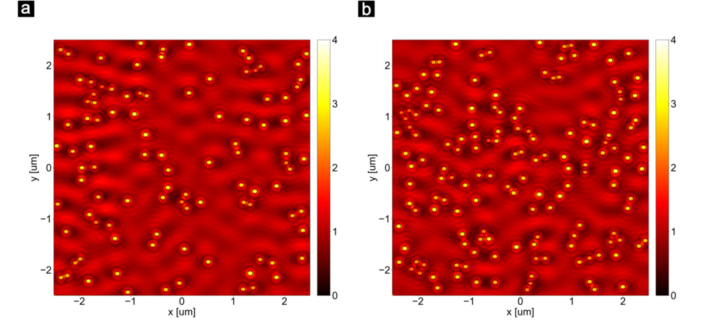
Figure 2. Local absorption enhancement in a 1 nm thick MoS2 layer on top of a gold film, calculated with Smuthi for the case of (a) N = 100 and (b) N = 150 randomly distributed 50 nm radius gold nanoparticles on top of the MoS2 layer. The total absorption enhancement inside MoS2 for the 5 um x 5 um area is around 18 % for (a) and 23 % for (b).
We also use Smuthi, a T-matrix based method Python package developed by Amos Egel for simulating light scattering on disordered layers in organic light emitting diodes [2]. For problems involving spheroidal and cylindrical particles, Smuthi relies on the NFM-DS Fortran code [3]. Here we consider ensembles of randomly distributed spherical nanoparticles on nanometer thick transition metal dichalcogenides, such as MoS2. In the examples shown in Figs. 2(a) and 2(b), we consider a 1 nm thick layer of MoS2 on top of a gold substrate with 50 nm radius gold nanoparticles randomly distributed on top. The plotted area shows the MoS2 absorption enhancement calculated for N = 100 and N = 150 gold nanoparticles distributed over a 5 um x 5 um area. As can be seen from the depicted maps, the absorption enhancement under a particle (indicated by a black circle) is strongly dependent on the entire ensemble. Thus, by investigating the fields and absorption enhancements in case of one or more particles, we hope to gain an understanding of how does the absorption enhancement depend on the particle size, distribution density and the structure of underlying layers.
In both COMSOL and Smuthi simulations shown above, experimental values of material permittivities were used for gold and silver [4] and monolayer MoS2 [5].
[1] B. Gallinet, J. Butet, O. J. F. Martin, “Numerical methods for nanophotonics: standard problems and future challenges,” Laser & Photonics Reviews 9, 577 (2015).
[2] A. Egel, “Accurate optical simulation of disordered scattering layers for light extraction from organic light emitting diodes,” Dissertation, Karlsruhe (2018).
[3] SCATTPORT NFM-DS URL: https://scattport.org/index.php/programs-menu/t-matrix-codes-menu/239-nfm-ds (Accessed online on April 10, 2021)
[4] A. D. Rakić et al., “Optical properties of metallic films for vertical-cavity optoelectronic devices,” Applied Optics 37, 5271 (1998)
[5] W. Li et al., “Broadband optical properties of large-area monolayer CVD molybdenum disulfide,” Physical Review B 90, 195434 (2014).